
PCB Design, Layout & PCBA Engineering Services
From schematic development and complex PCB layout to manufacturing coordination and in-house SMT assembly, Excel Circuit supports high-speed, HDI, RF, FPGA, embedded and power electronics projects from design to production.
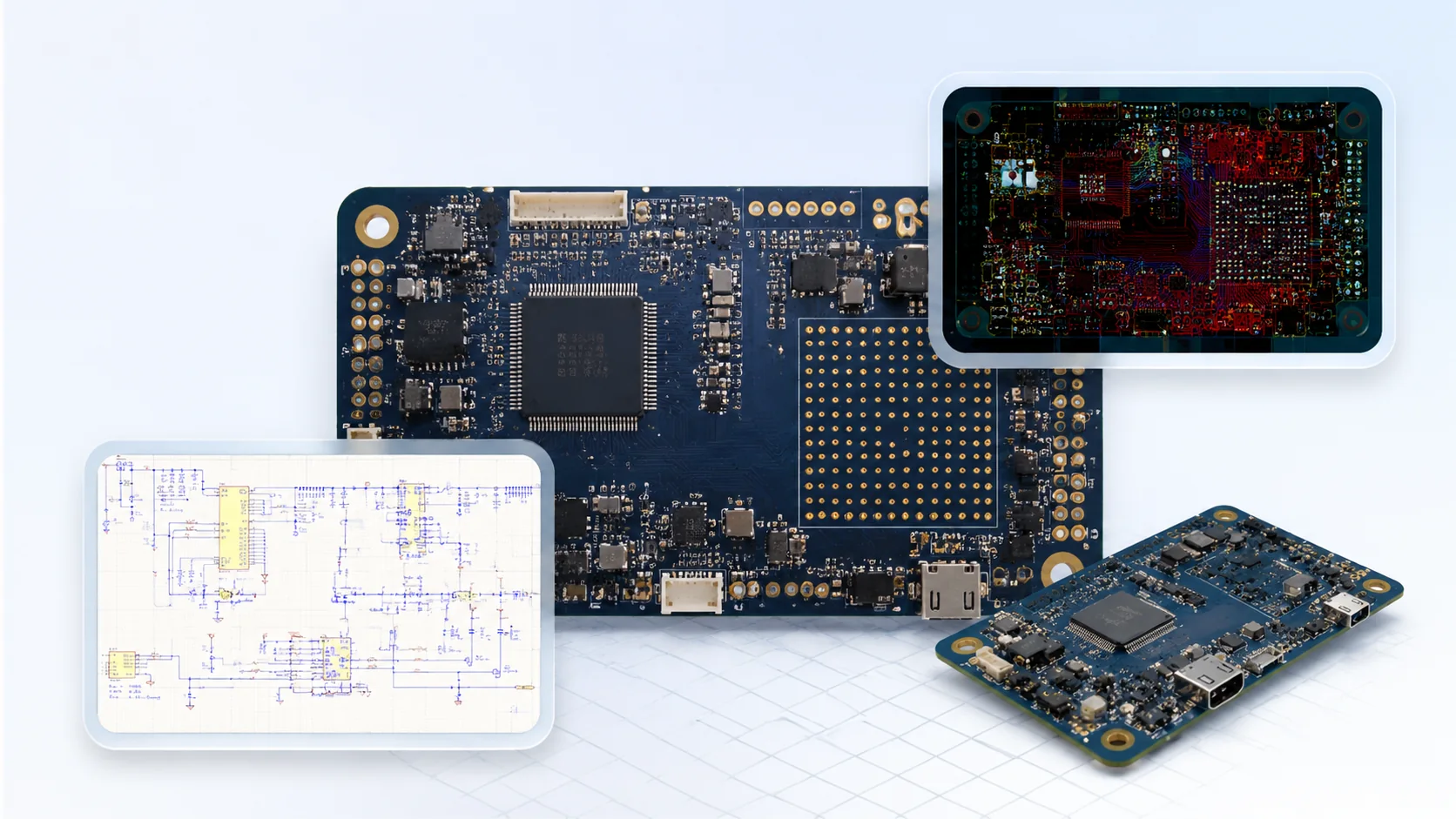
Key Engineering Metrics
Layers
Maximum PCB Design Layers
Minimum Trace / Space
High-Precision PCB Design
RF & High-Frequency Design
High-Frequency Engineering Support
Minimum BGA Pitch
Fine-Pitch BGA Layout Capability
Pin BGA
High-Density BGA Design Capability
EDA Design Tools
Professional PCB layout support across major industry-standard EDA environments.
Altium Designer
Cadence Allegro
Siemens PADS
Siemens Xpedition
Prototype from 5 pcs
Flexible prototype assembly for engineering validation and early production builds.
Free DFM / DFA Analysis
Manufacturability and assembly risks can be reviewed before production release.
Engineering & Production Capabilities
From complex PCB layout to fabrication coordination and in-house SMT assembly, engineering and production support are connected within one project workflow.
PCB Design & Layout Engineering
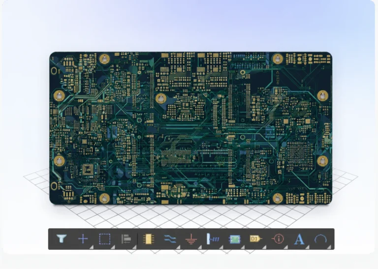
- Multilayer & HDI PCB layout
- Fine-pitch BGA fanout
- Controlled impedance & differential routing
- SI / PI & production-ready design considerations
Qualified PCB Manufacturing Support
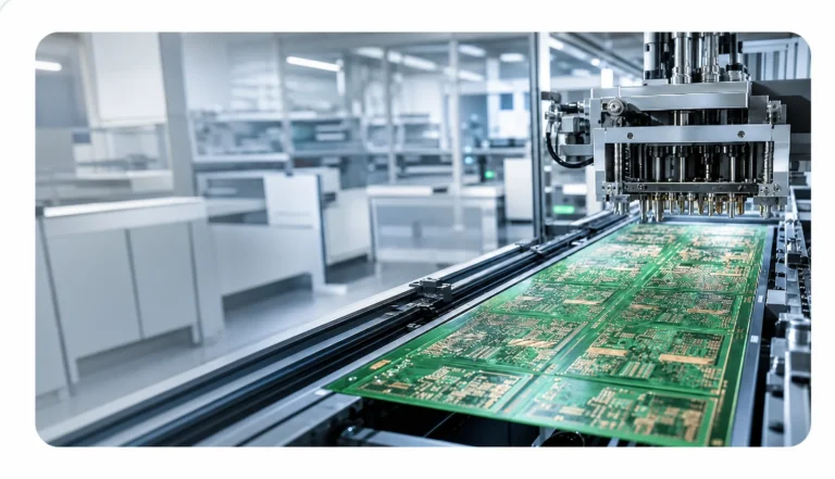
- Qualified PCB manufacturing resources for high-layer-count & HDI PCB
- Controlled-impedance fabrication
- RF material & advanced via support
- Rigid-flex / heavy-copper options where required
In-House SMT Assembly
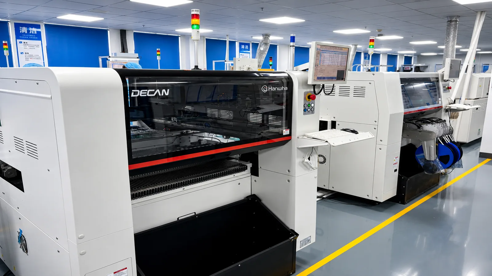
- Prototype SMT turnaround as fast as 2–3 days
- Prototype & low-volume assembly
- BGA / QFN / fine-pitch assembly
- Reflow, AOI & X-ray where required
Engineering Expertise Behind Every PCB Design
Work with PCB layout, DFM/DFA and SMT process engineering support throughout design review and prototype production.

PCB Layout Engineer
Supports placement, routing and layout decisions for complex multilayer PCB projects while coordinating design constraints with production requirements.
Layout · Routing · Stackup Coordination

DFM / DFA Engineer
Reviews design and production data for manufacturability and assembly risks before PCB files are released for fabrication and SMT.
DFM · DFA · Production Readiness

SMT Process Engineer
Supports prototype assembly planning and process review as PCB designs move from fabrication into in-house SMT production.
SMT Process · Prototype Assembly · Inspection Coordination
Advanced PCB Design & Layout Engineering
Engineering support for complex multilayer PCB layouts involving high-speed interfaces, HDI structures, dense BGA routing, signal and power integrity, impedance control and production-ready design constraints.
High-Speed Signal Design
High-speed routing coordinates impedance control, differential pairs, length matching and stable reference-plane planning.
- High-speed interface routing
- Differential-pair length matching
- Controlled-impedance planning
HDI & Advanced Via Design
HDI routing uses blind and buried vias, microvias and via-in-pad structures for dense multilayer PCB layouts.
- Blind & buried via structures
- Microvia routing strategy
- Via-in-pad implementation
BGA Fanout & Escape Routing
BGA fanout and escape routing coordinate dense packages, routing channels and multilayer layer allocation.
- Dense BGA fanout planning
- Escape-routing channel design
- Multilayer layer allocation
Signal Integrity & Return Paths
Signal-integrity routing considers return paths, reference planes, crosstalk and timing relationships.
- Return-path continuity
- Reference-plane strategy
- Crosstalk & timing control
Power Integrity & PDN Design
Power-integrity planning coordinates decoupling, power distribution, grounding and current return paths.
- PDN & decoupling strategy
- Power-distribution planning
- Ground & current-return paths
Stackup, Thermal & EMI Design
PCB stackup, copper distribution, grounding and thermal layout are coordinated with EMI/EMC constraints.
- Layer-stack planning
- Thermal & high-current paths
- EMI / EMC-oriented layout
Typical PCB Layout Lead Time
Typical PCB layout schedules vary with design complexity, pin count, stackup, high-speed interfaces and mechanical constraints. The ranges below provide a practical reference for project planning.
Pin Count
Typical Lead Time
< 1,000 pins
3–5 working days
2,000–3,000 pins
5–7 working days
4,000–5,000 pins
8–12 working days
6,000–9,000 pins
15–18 working days
10,000–13,000 pins
18–20 working days
14,000–15,000 pins
20–22 working days
16,000–20,000 pins
22–30 working days
Planning note: These are typical engineering lead-time ranges rather than guaranteed delivery dates. Final schedules depend on PCB complexity, layer count, interface requirements, component density, mechanical constraints and customer review cycles.
Projects falling between the reference pin-count ranges are quoted individually.
Free DFM & DFA Review Before Production
Review key design, fabrication and assembly risks before PCB files are released for production.
01
Design Verification
Review PCB design data, electrical requirements and layout constraints before manufacturing release.
- Schematic & footprint consistency
- Stackup & impedance requirements
- Critical PCB design constraints
02
Manufacturing Verification
Check PCB production data against practical fabrication rules and manufacturability requirements.
- Trace / space requirements
- Drill & via checks
- Fabrication clearance review
03
Assembly Verification
Review component and placement data for potential assembly issues before prototype production.
- BOM & package matching
- Component placement & polarity
- Assembly readiness review
Free engineering analysis before production. NDA available before confidential project files are reviewed.
Review scope is determined by the project files and manufacturing requirements provided.
Have Gerber, BOM or PCB source files ready? Send them for engineering review.
From Concept to Production
01
NDA & Requirement Review
Review project requirements, schematic data, BOM, mechanical constraints and available PCB files before engineering work begins.
NDA · Requirements · Engineering Files
02
PCB Design & DFM/DFA
Develop PCB placement and routing while considering stackup, impedance, manufacturability and assembly requirements before production release.
PCB Layout · DFM/DFA · Design Review
03
Customer Review & Sign-Off
Review the engineering output with the customer and confirm the production package before fabrication and assembly.
Review · Feedback · Release Approval
04
PCB Fabrication & In-House SMT
Coordinate PCB fabrication through qualified manufacturing resources, followed by component sourcing and in-house SMT assembly.
PCB Fabrication · Sourcing · In-House SMT
05
Inspection & Delivery
Inspect assembled boards according to project requirements before final release and delivery.
Inspection · Final Review · Delivery
Component Sourcing & BOM Control
Component sourcing support combines BOM review, availability checks and controlled part substitution for prototype and PCBA projects.
BOM & Sourcing Review
Review BOM data, manufacturer part numbers, package information and component availability before procurement and assembly.
- Manufacturer part number
- Package / footprint consistency
- BOM completeness
- Availability & lead-time review
Supply & Substitution Control
Alternative parts and incoming components are reviewed against project requirements before use in prototype or PCBA production.
- Alternative MPN review
- Package / electrical compatibility
- Customer approval before substitution
- Incoming part verification
Component sourcing is available for prototype and PCBA projects. Any proposed part substitution requires customer confirmation where applicable.
PCB Engineering for Diverse Hardware Applications
PCB engineering support for embedded, industrial, RF, power, connected and mixed-signal hardware applications.
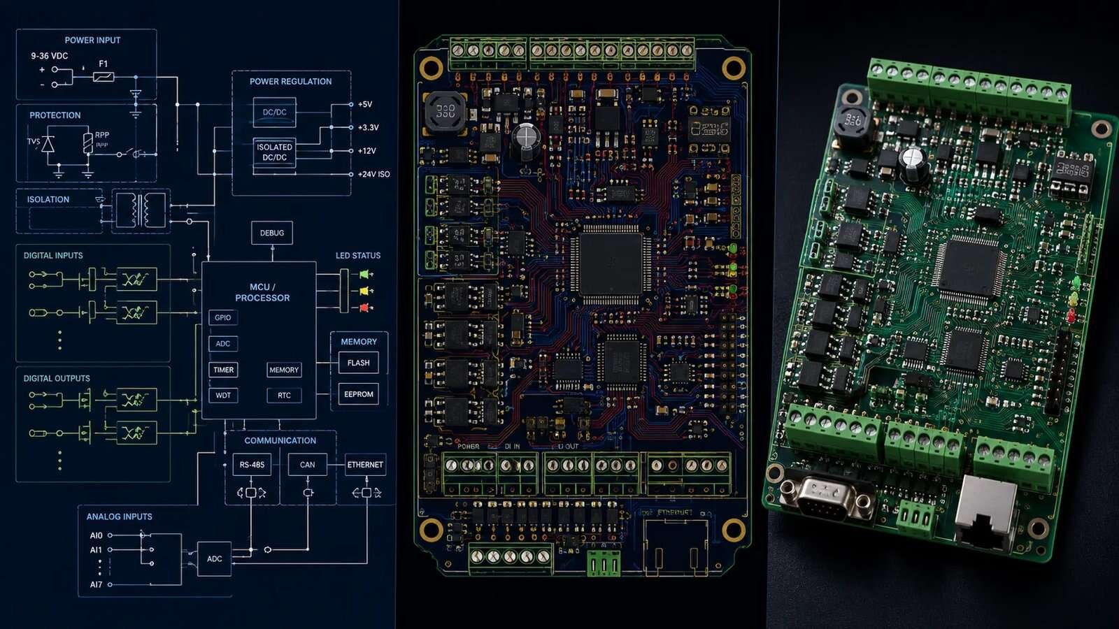
Embedded & FPGA Systems
PCB layout support for FPGA, processor, memory and embedded-control hardware with dense digital routing requirements.
Industrial Electronics
PCB engineering for controllers, communication interfaces, sensing electronics and embedded industrial control systems.
RF & Wireless Devices
PCB layout support for RF-sensitive and wireless hardware requiring careful impedance, grounding and signal-path planning.
Power Electronics
PCB design support for power-conversion and high-current circuitry with attention to current paths, copper distribution and thermal behavior.
IoT & Connected Hardware
Compact PCB engineering for connected devices combining embedded processing, sensors, wireless modules and power management.
Analog & Mixed-Signal Systems
PCB layout support for analog, digital and power sections requiring careful grounding, partitioning and noise-sensitive routing.
Why Engineering Teams Work With Excel Circuit
Engineering-first collaboration, prototype flexibility and connected design-to-production support help reduce handoffs throughout hardware development.
Direct Engineering Collaboration
Discuss design constraints and production requirements around the engineering issues that affect your PCB project.
Prototype-Friendly Support
Support for engineering prototypes and low-volume builds, including in-house SMT assembly from 5 pcs.
Design-to-Production Continuity
PCB design, qualified fabrication resources, component sourcing and in-house SMT assembly are coordinated within one project workflow.
Confidential Project Handling
NDA arrangements are available before confidential PCB design files are reviewed.
QUALITY ASSURANCE
Engineering Quality You Can Verify
From PCB design review and qualified manufacturing resource management to in-house SMT assembly, inspection and traceability, our quality controls are designed around production readiness, repeatability and reliable PCBA delivery.
Explore how engineering review, sourcing control, SMT process inspection and documentation work together throughout the project lifecycle.
QUALITY ASSURANCE
Quality Assurance Whitepaper
PCB Design → PCBA Delivery
Engineering review · Sourcing control · SMT inspection · Traceability
Featured PCB Engineering Examples
Representative PCB engineering scenarios illustrating design challenges, layout decisions and prototype planning across different hardware applications.
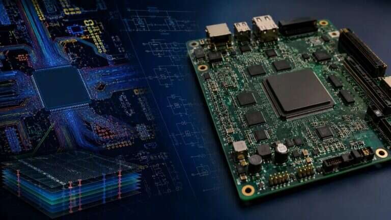
REPRESENTATIVE ENGINEERING EXAMPLE
FPGA & Embedded Design Example
Dense pin fields, multiple power domains and timing-sensitive interfaces require coordinated placement, BGA escape and power distribution.
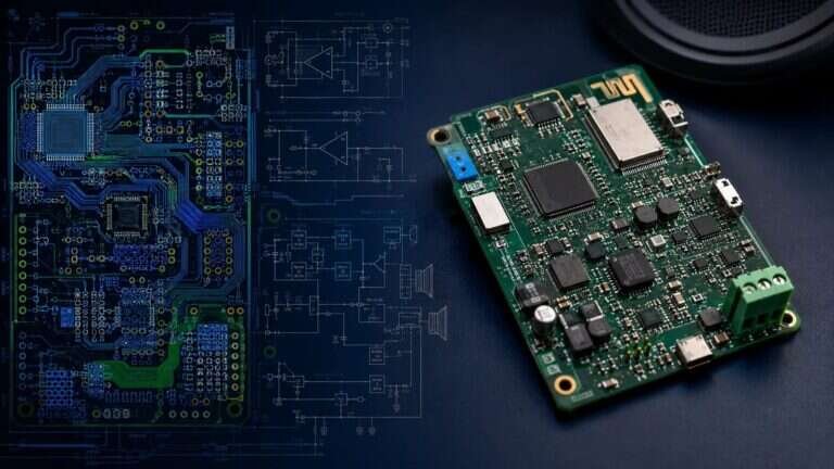
REPRESENTATIVE ENGINEERING EXAMPLE
Bluetooth Audio Hardware Example
Wireless, digital-control, analog-audio and switching-power sections require careful partitioning for noise control and prototype bring-up.
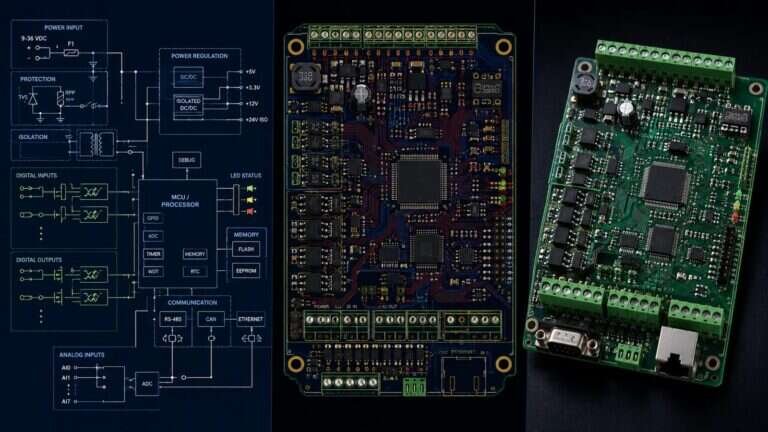
REPRESENTATIVE ENGINEERING EXAMPLE
Industrial Controller Board Example
Protected field I/O, embedded processing and industrial communications require clear protection, grounding and isolation planning.
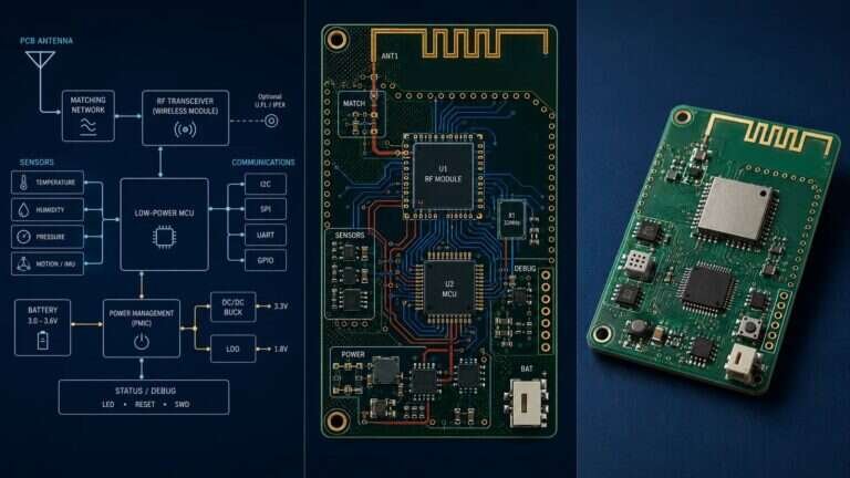
REPRESENTATIVE ENGINEERING EXAMPLE
RF & IoT Board Example
Antenna clearance, controlled RF geometry, sensor integrity and low-power design must be coordinated with enclosure constraints.
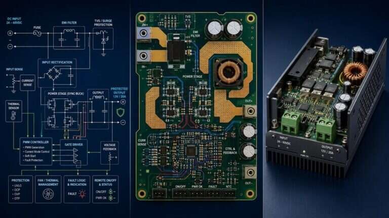
REPRESENTATIVE ENGINEERING EXAMPLE
Power Electronics Board Example
High current, switching edges and heat generation require short current loops, planned copper geometry and thermal strategy.
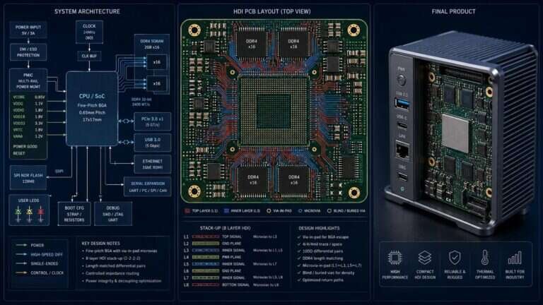
REPRESENTATIVE ENGINEERING EXAMPLE
HDI & Fine-Pitch BGA Example
Fine-pitch escape requires coordinated pad structures, microvia strategy, multilayer stack-up and manufacturability review.
PCB Engineering Resources
Practical engineering guides covering high-speed routing, BGA design, FPGA power integrity and RF PCB development.
DDR PCB Routing Guidelines
Practical routing considerations for DDR interfaces, including signal paths, timing relationships, reference planes and layout decisions that influence high-speed PCB performance.
BGA Fanout Design Guide
Learn how BGA fanout, escape routing, via strategy and layer planning influence routing density in complex PCB layouts.
FPGA Power Integrity
Explore decoupling, power distribution and PCB layout considerations for stable FPGA power delivery in dense embedded hardware designs.
RF PCB Design
Review RF PCB layout considerations involving impedance, grounding, signal paths and routing decisions for frequency-sensitive hardware.