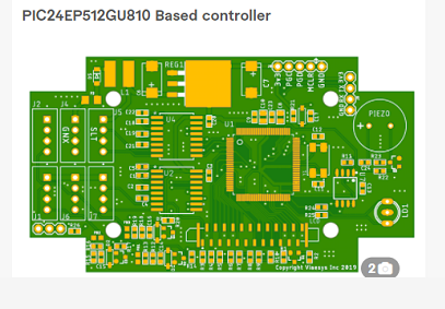
In the ever-evolving world of electronics, efficient and reliable circuit board design is crucial. A well-designed printed circuit board (PCB) layout can significantly impact the performance, functionality, and manufacturability of electronic devices. By optimizing the PCB layout, you can unlock the true potential of your electronics design, leading to improved product quality, reduced costs, and faster time-to-market. In this article, we will explore the importance of PCB layout and discuss key strategies for maximizing its benefits.
**Why PCB Layout Matters**
A PCB serves as the foundation for electronic components, connecting various elements and enabling their seamless operation. The PCB layout plays a pivotal role in determining how signals flow through the circuit, minimizing noise, and ensuring the efficient transfer of power. A poorly designed layout can result in signal integrity issues, electromagnetic interference (EMI), and thermal problems, compromising the overall functionality and reliability of the device.
**Optimizing Signal Integrity**
Signal integrity is a critical aspect of any electronics design. Achieving high signal integrity requires careful consideration of various factors during PCB layout. One of the primary considerations is the proper placement of components to minimize signal distortion and interference. Grouping related components together and positioning them closer to each other reduces the length of signal traces, decreasing the chances of signal degradation.
Additionally, employing a multilayer PCB design allows for separate power and ground planes, which act as shielding layers, reducing noise and providing a stable reference for signals. This approach helps mitigate crosstalk, EMI, and power integrity issues.
**Thermal Management**
Effective thermal management is essential for ensuring the longevity and reliability of electronic devices. Heat dissipation is a significant concern, especially for power-intensive applications or densely packed circuits. A well-designed PCB layout incorporates proper placement of heat-generating components, such as power regulators and high-power ICs, in proximity to heat sinks or thermal vias for efficient heat dissipation.
The strategic arrangement of components and the use of copper pours or planes as thermal reliefs aid in conducting heat away from sensitive components, preventing thermal hotspots. Thermal vias, placed strategically, allow heat to be conducted through the PCB layers, facilitating effective heat dissipation.
**Manufacturability and Cost Reduction**
Efficient PCB layout design not only improves functionality but also enhances manufacturability and reduces production costs. A well-optimized layout takes into account the capabilities and limitations of the manufacturing processes, ensuring that the PCB can be manufactured efficiently and reliably.
Considerations such as component placement, orientation, and routing complexity influence the ease of assembly, inspection, and testing. By minimizing the need for complex manual interventions during manufacturing, you can streamline the production process and reduce the chance of errors, leading to cost savings and improved time-to-market.
**Design for Testability**
Designing PCBs with testability in mind is crucial for effective quality control and troubleshooting. Incorporating test points, such as test pads or vias, at critical locations facilitates electrical testing and debugging during the manufacturing process. Strategic placement of these test points enables easy access to key signals, allowing for efficient and accurate testing, reducing production time and minimizing the risk of faulty devices reaching the market.
**Collaborative PCB Design Tools**
To harness the full potential of PCB layout optimization, it is essential to leverage modern collaborative PCB design tools. Advanced design software offers a wide range of features, including schematic capture, component libraries, and interactive routing capabilities. These tools enable seamless collaboration among engineers, streamlining the design process and ensuring efficient communication of design intent.
Additionally, many PCB design tools provide design rule checks (DRCs) and simulation capabilities, allowing engineers to validate the design for electrical, thermal, and manufacturing constraints. By utilizing these features, potential issues can be identified and

