Contents
1. Patch device spacing
This article sorts out some details that need to be paid attention to in Layout, let’s see whether you know them all !
The spacing between SMD components is a problem that engineers must pay attention to
during layout. The spacing between SMDs can neither be too large (wasting the circuit
layout) nor too small to avoid solder paste printing adhesion and soldering repair difficulties.

The spacing size can refer to the following specifications:
Same kind of devices: ≥0.3mm
Dissimilar devices: ≥0.13*h+0.3mm (h is the maximum height difference of neighboring
components)
When manual soldering and patching, the distance between the devices is required: ≥ 1.5mm
2. The distance between the in-line device and the patch

As shown in the figure above, a sufficient distance should be maintained between the in-line resistance device and the patch, and it is recommended to be between 1-3mm. Due to the troublesome processing, the use of straight plug-ins is rare now.
3. The placement direction and distance of the edge devices of the board
Since

Since the PCB is generally made of jigsaw, the devices near the edge need to meet two conditions.
- (1) Parallel to the cutting direction. Make the mechanical stress of the device uniform. For example, if the device is placed in the way on the left side of the above figure, the different force directions of the two pads of the patch may cause the component and the pad to fall off when the puzzle is to be split.
- (2) Devices cannot be arranged within a certain distance to prevent damage to the components when the board is cut.
4. Consistent lead width of components

5. Device decoupling rules Add

Add necessary decoupling capacitors on the printed plate to filter out interference signals on the power supply and stabilize the power supply signal. It is recommended that the power supply be connected to the power supply pin after passing through the filter capacitor.
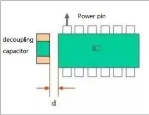
6. Placement of IC’s decoupling capacitors

Decoupling capacitors need to be placed near the power port of each IC, and the location should be as close as possible to the power port of the IC.
When a chip has multiple power ports, a decoupling capacitor must be arranged for each port.
7. Placement of the crystal oscillator
The crystal oscillator is composed of quartz crystal, which is easily affected by external impact or drop. Therefore, it is best not to place it on the edge of the PCB and to place it as close to the chip as possible during layout.
The placement of the crystal oscillator needs to be far away from the heat source, because high temperature will also affect the frequency deviation of the crystal oscillator.
8. Layout of special components
8-1. Special high-frequency components should be placed next to each other to shorten the
connection between them;
8-2. Sensitive components should be kept away from noise sources such as clock generators
and oscillators;
8-3. The layout of adjustable components such as adjustable inductors, variable capacitors,
key switches, potentiometers, etc. should meet the structural requirements of the whole
machine and facilitate adjustment;
8-4. Heavier components should be fixed with brackets;
8-5. The EMI filter should be placed close to the EMI source.
9. Keep electrolytic capacitors away from heat sources
When designing, the PCB engineer must first consider whether the ambient temperature of the electrolytic capacitor meets the requirements, and secondly, keep the capacitor as far away from the heating area as possible to prevent the liquid electrolyte inside the electrolytic capacitor from being dried.
10. Keep unused pin pads

For example, in the picture above, two pins of a chip do not need to be used, but the physical pins of the chip exist. If the two pins on the right side of the picture above are in a floating state, it is easy to cause interference.
If the chip pin itself is not connected inside, adding a pad and then grounding the pad to shield it can avoid interference.
11. Use vias with caution
In almost all PCB layouts, vias must be used to provide conductive connections between different layers. PCB design engineers need to be especially careful, because vias will generate inductance and capacitance. In some cases, they will also produce reflection, because the characteristic impedance will change when the via is made in the trace.
Also keep in mind that vias will increase the length of the trace and need to be matched. If it is a differential trace, avoid vias as much as possible; if it cannot be avoided, use vias in both traces to compensate for the delay in the signal and return path.
12. It is best not to punch the vias on the pads

It is best not to punch the via hole on the pad, which is easy to cause solder leakage.
13. Adjacent pads connected

If adjacent pads need to be connected, first confirm that the connection is made outside to prevent bridging caused by the connection, and pay attention to the width of the copper wire at this time.
14. When the pad falls in a common area, heat dissipation needs to be considered
If the pad falls on the pavement area, the right way should be used to connect the pad and pavement. Also, determine whether to connect 1 wire or 4 wires according to the current.

If the method on the left is adopted, it is more difficult to weld or repair and disassemble the components, because the temperature is fully dispersed by the copper laid, which makes the welding impossible.
15. Leads<plug-in pads need to add teardrops

If the wire is smaller than the pad of the in-line device, you need to add teardrops as shown on the right side of the figure.
Adding teardrops has the following benefits:
Avoid the sudden decrease of the signal line width and cause reflection, which can make the connection between the trace and the component pad tend to be smooth and transitional.
The problem that the connection between the pad and the trace is easily broken by impact is solved.
The setting of teardrops can also make the PCB circuit board look more beautiful.