Category: PCB Info

PCB Info

210814-Specializes in high multilayer PCB, rigid flex PCB, HDI PCB

Excel Circuit, which specializes in high multilayer PCB, rigid flex PCB, HDI PCB. Cares about customer’s benefit with high quality, high efficiency and lower cost is the best advantage we excel in market. Material available: (A) FR-4 : Sheng Yi, KingBoard, ITEQ ,370HR,TU768,EM285,EM370 (B) Alu base : TOTKING, BoYu, Bergquist (C) PTFE & Ceramic : Rogers RO4350B, RO4003C (D) PI Material:SYE(1-2mil) Panasonic(1-4mil)Dupont(1-4mil) Laminate: FR4, Aluminum base, PTFE, Ceramic etc. FR4 Thickness: 0.25mm-6.5mm FR4 Copper thickness: 1/2oz ~ 12oz PCB Services – Quick PCB Proto-typing, Single Sided PCB, Double Sided PCB, Multilayer PCB up to 40 Layers, Aluminum PCB, High Temperature PCB, Flex PCB, Flex-Rigid PCB. PCB Assembly Services – Hand Build Assembly, Pick & Place Assembly, Through Hole Assembly, Surface Mount Assembly (SMT), BGA Assembly + X-Ray. Any needs for PCB and PCBA, pls contact me. A reliable supplier can serve you better. My contact information: sales2@excelcircuit.com whatsapp:+86-15364019151 Skype: phm1989@sina.com

Read More »
PCB Info

The Details Determine Success or Failure 15 Points for Attention in PCB Design

1. Patch device spacing This article sorts out some details that need to be paid attention to in Layout, let’s see whether you know them all !The spacing between SMD components is a problem that engineers must pay attention toduring layout. The spacing between SMDs can neither be too large (wasting the circuitlayout) nor too small to avoid solder paste printing adhesion and soldering repair difficulties. The spacing size can refer to the following specifications:Same kind of devices: ≥0.3mmDissimilar devices: ≥0.13*h+0.3mm (h is the maximum height difference of neighboringcomponents)When manual soldering and patching, the distance between the devices is required: ≥ 1.5mm 2. The distance between the in-line device and the patch As shown in the figure above, a sufficient distance should be maintained between the in-line resistance device and the patch, and it is recommended to be between 1-3mm. Due to the troublesome processing, the use of straight plug-ins is rare now. 3. The placement direction and distance of the edge devices of the boardSince Since the PCB is generally made of jigsaw, the devices near the edge need to meet two conditions. (1) Parallel to the cutting direction. Make the mechanical stress of the device uniform. For example, if the device is placed in the way on the left side of the above figure, the different force directions of the two pads of the patch may cause the component and the pad to fall off when the puzzle is to be split. (2) Devices cannot be arranged within a certain distance to prevent damage to the components when the board is cut. 4. Consistent lead width of components 5. Device decoupling rules Add Add necessary decoupling capacitors on the printed plate to filter out interference signals on the power supply and stabilize the power supply signal. It is recommended that the power supply be connected to the power supply pin after passing through the filter capacitor. 6. Placement of IC’s decoupling capacitors Decoupling capacitors need to be placed near the power port of each IC, and the location should be as close as possible to the power port of the IC. When a chip has multiple power ports, a decoupling capacitor must be arranged for each port. 7. Placement of the crystal oscillator The crystal oscillator is composed of quartz crystal, which is easily affected by external impact or drop. Therefore, it is best not to place it on the edge of the PCB and to place it as close to the chip as possible during layout. The placement of the crystal oscillator needs to be far away from the heat source, because high temperature will also affect the frequency deviation of the crystal oscillator. 8. Layout of special components 8-1. Special high-frequency components should be placed next to each other to shorten theconnection between them; 8-2. Sensitive components should be kept away from noise sources such as clock generatorsand oscillators; 8-3. The layout of adjustable components such as adjustable inductors, variable capacitors,key switches, potentiometers, etc. should meet the structural requirements of the wholemachine and facilitate adjustment; 8-4. Heavier components should be fixed with brackets; 8-5. The EMI filter should be placed close to the EMI source. 9. Keep electrolytic capacitors away from heat sources When designing, the PCB engineer must first consider whether the ambient temperature of the electrolytic capacitor meets the requirements, and secondly, keep the capacitor as far away from the heating area as possible to prevent the liquid electrolyte inside the electrolytic capacitor from being dried. 10. Keep unused pin pads For example, in the picture above, two pins of a chip do not need to be used, but the physical pins of the chip exist. If the two pins on the right side of the picture above are in a floating state, it is easy to cause interference. If the chip pin itself is not connected inside, adding a pad and then grounding the pad to shield it can avoid interference. 11. Use vias with caution In almost all PCB layouts, vias must be used to provide conductive connections between different layers. PCB design engineers need to be especially careful, because vias will generate inductance and capacitance. In some cases, they will also produce reflection, because the characteristic impedance will change when the via is made in the trace. Also keep in mind that vias will increase the length of the trace and need to be matched. If it is a differential trace, avoid vias as much as possible; if it cannot be avoided, use vias in both traces to compensate for the delay in the signal and return path. 12. It is best not to punch the vias on the pads It is best not to punch the via hole on the pad, which is easy to cause solder leakage. 13. Adjacent pads connected If adjacent pads need to be connected, first confirm that the connection is made outside to prevent bridging caused by the connection, and pay attention to the width of the copper wire at this time. 14. When the pad falls in a common area, heat dissipation needs to be considered If the pad falls on the pavement area, the right way should be used to connect the pad and pavement. Also, determine whether to connect 1 wire or 4 wires according to the current. If the method on the left is adopted, it is more difficult to weld or repair and disassemble the components, because the temperature is fully dispersed by the copper laid, which makes the welding impossible. 15. Leads<plug-in pads need to add teardrops If the wire is smaller than the pad of the in-line device, you need to add teardrops as shown on the right side of the figure. Adding teardrops has the following benefits: Avoid the sudden decrease of the signal line width and cause reflection, which can make the connection between the trace and the component pad tend to be smooth and transitional. The problem that the connection between the pad and

Read More »
PCB Info

What should be paid attention to in the processing of medical electronic SMT patches?

What matters should be paid attention to in the processing of medical electronic SMT patches, medical electronic products have their own special requirements: Whether it is medical testing equipment or medical auxiliary tools and equipment, it needs to be very high in use, and things about life cannot be approximated, left or right, and so on. High stability: Especially for medical diagnosis and medical auxiliary tools and equipment, high stability is essential, the diagnosis in the diagnosis stage, the stability of the application in the clinical application stage. Taking into account the special requirements of medical equipment, for medical electronics SMT patch processing plants, it is necessary to strengthen the quality control of SMT patch processing. Quality control of components: For the control of medical electronic components, first of all, we must control the quality from the source of procurement. After the purchase is completed, IPQC needs to conduct a full inspection of the components, seal the samples and store them, and special BGA and IC must be stored in a moisture-proof cabinet. Solder paste control: The patch processing of medical electronics must select and store solder paste according to the characteristics of the product. The stirring and the addition of flux in the application process must be strictly controlled. Solder joint control: After the quality of components and solder paste is completely OK, the control of solder joints determines the quality of SMT chip processing. Simply put, the quality of solder joints determines the quality of chip processing. Static electricity control: The instantaneous discharge of static electricity can reach several thousand/w. The damage to BGA and IC components is invisible and potential damage. Medical electronics need to deal with considerable data in the application. If the core components are damaged by static electricity, they will be lost. Stability will affect the stability of the product. In addition, in the SMT patch processing of medical electronics, there are not only the above four points, but also many aspects that require manufacturers to work hard. To be truly responsible for the product and the user of the product is a problem that the manufacturer must face.

Read More »
PCB Info

What is BOM DIP SMT SMD?

SMT patch processing term explanation: what is BOM, DIP, SMT, SMD In the 1980s, the SMT production process became more and more perfect. The mass production and manufacture of components used for surface mounting technology was greatly reduced. Various types of equipment with good technical performance and low prices were successively available. Electronic equipment assembled by SMT is available. Small size, good performance, complete functions, and low price advantages, so SMT, as a new generation of electronic assembly technology, is widely used in aviation, aerospace, communications, computers, medical electronics, automobiles, office automation, household appliances and other fields The electronic equipment is installed in the United States. Next, let’s take a look at the explanation of SMT patch processing terms: what is BOM, DIP, SMT, and SMD.

Read More »
PCB Info

How the PCB is produced?

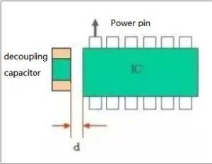
Although PCB is already well-known, it can even be said that we deal with it every day. So, what exactly is it? How is it produced? How many production processes are there? Let’s walk into the PCB manufacturing factory in Shenzhen, China for some exploration! 2. The production process of PCB 2.1 Design board receiving and inspection The engineering department of the factory accepts and checks the design board file sent by the customer. The contents of the inspection include: whether the design document is appropriate, whether the layer is missing, ensuring that there is a border on the file, whether the drilling file exists, etc. If the design is flawed, the engineering department will inform the designer to modify it. If there is no design problem, mass production can be carried out according to the design. 2.2 Print the design into transparencies Print the checked design documents into transparencies. The light is projected onto these films, and the photoresist is exposed on the circuit board in a way similar to exposing photos. The design of the circuit boards is like a movie, lifelike and particularly vivid. 2.3 Cutting and edge polishing of glass fiber The glass fiber is selected and cut and polished. Select FR-4 type glass fiber with copper plated on the top and bottom layers, and then cut the designed size on the cutting machine. Because the edge of the glass fiber is too rough, we need to polish its edge. 2.4 Inner layer production The top and bottom layers of glass fiber are covered with plastic dry film and are hardened under UV exposure. After the two sides of the glass fiber are hardened with dry film, the machine is used to press them together, which can effectively prevent the copper from being dissolved by the alkaline liquid in the subsequent process. 2.5 Etching process The purpose of the entire etching process is to remove excess copper and photoresist from the copper plate, and complete the prototype of the PCB after a series of processes. Remove excess copper and photoresist from the laminated glass fiber, complete the etching process through the baptism of alkaline solution, and finally complete the entire etching process through the combination of film removal, washing, drying, and drying. 2.6 Automatic optical inspection (AOI) and editing vacuum (PP) The purpose of automatic optical inspection is to check the etching of the inner layer to ensure that the etching of the inner layer is normal. Attach a yellow patch similar to epoxy to both sides of the board to increase the bonding force. 2.7 High temperature and high pressure treatment After 200 degrees Celsius and 27 kilograms of pressure, the epoxy resin in the melted prepreg glues the PCB board on both sides to complete the lamination. 2.8 Drilling technology Drilling is to use a machine that automatically replaces the drill bit to drill out the required holes according to the design. There are three types of holes on the PCB board: through holes, blind buried holes, and mechanical holes. In this step of drilling, holes can be punched out as needed to facilitate subsequent operations such as welding of components. 2.9 Electroplating process Electroplating requires a very complete chemical process to be completed. After drilling, the areas without copper are plated with copper, so that the PCB can be turned on, and then the copper in the hole is thickened again, because the plating is not thick at one time and requires multiple operations. 2.10 Solder mask and drying The electroplated PCB board needs another automatic optical inspection (AOI) before it can be painted with a green liquid solder mask and then dried. When it comes to the color of the PCB board, everyone’s first reaction is definitely green, so how did it come from? The secret lies in the solder mask. 2.11 Welding mask removal, washing and screen After the removal, the solder mask needs to be cured. After keeping the original shape, we need to wash off the unnecessary things, remove the pads of the circuit board, and finally paste the silk screen for the customers in need. 2.12 Hot air treatment (HASL) Hot air processing involves immersing the circuit board in liquid solder, and after pulling it out, blow off the excess with a hot air sheet. 2.13 PCB cutting Since there are many different small pieces on each large PCB, they come from many different customers. Therefore, we need to cut it. 2.14 Short circuit and open circuit test Do you think this is over? NO! NO! NO! There is also the most important link. We need to perform short-circuit and open-circuit tests on the circuit boards to ensure that each circuit board can conduct normally. The miniature robotic arm quickly verifies the electrical connection between the two pads, one after the other, which is really incredible. 2.15 Packaging and shipping PCB packaging and transportation are also very particular. After a series of processes such as sorting, packaging, and labeling are completed, they can be shipped to customers. Generally, customers can complete the order within 24 hours after placing an order. For domestic orders, it can be delivered within 1-2 days, and for international orders, it takes about a week. 3. Summary After reading the above sharing, you must have discovered that the factory production of PCB boards has a total of about 15 processes, whether it feels particularly complicated. In fact, with the development of science and technology, many jobs that require manpower are slowly being replaced, and the industrial system and industrial technology are constantly being improved and updated. I believe that in the near future, the PCB industry will also have many new innovations. The PCB board has been made, so how are the miniature components soldered to the circuit board? We will announce the next issue, so stay tuned!

Read More »
PCB Info

The composition and main functions of the circuit board

The PCB is made of different components and a variety of complex process technologies. Among them, the structure of the PCB circuit board has a single-layer, double-layer, and multi-layer structure. The production methods of different hierarchical structures are different.

Read More »
PCB Info

How to reuse PCB design

The most common problem with headphones is with the plug. That’s the part that goes into your phone, computer, or sound system. It’s also the part that’s tugged the hardest and where a lot of connections are made, so think of it as an Achilles heel of sorts—the plug is the weakest link.

Read More »