- +86 15364019151
- sales2@excelcircuit.com
- Mon - Fri: 9:00 - 18:00
Business Introduction
Our goal is to train first-class employees, manufacture first-class products, build first-class enterprises, and jointly contribute to the development of the electronic industry
The senior layout design team
More than 10 years of professional design experience, providing solutions from design to manufacturing.
Difficult design experience
Good at high frequency, high speed, high density, digital-analog hybrid, high power, high current, radiofrequency, ATE, rigid-flex board, high-speed backplane, etc.;
Rich technical resources
Master the most advanced technical information, fully consider EMI, EMC, and design for manufacturability.
High quality management system
Standardized design and management system, strict inspection and check at every level, never let go of any mistakes and details.
High standards of confidentiality
A confidentiality agreement is signed; the company’s designer’s computer is fully encrypted, and all documents need to be approved for export.
Excel Circuit PCB design, Layout a perfect electronic artwork for you
Based on printed circuit board design and manufacturing services, actively create PCB design, PCB manufacturing, SMT patch, materials one-stop business.
Our Advantage
★-Provide customers with PCB packaging construction for free (customers provide device DataSheet)
★-Provide customers with PCB impedance calculation, laminated design, QA inspection, process inspection, EMC inspection for free
★-Innovative morning and evening shift operation mode, making full use of online and parallel operations to divide tasks to ensure design delivery
★-Set up a special discussion group for the project, engineers ensure real-time communication, and a dedicated person to follow up the progress to ensure the progress
★-Provide optimization solutions throughout the process, fully evaluate designability and manufacturability, and maximize the reduction of board manufacturing costs for customers
★-Convenient debugging for customers, considering issues such as post welding, and reducing unnecessary welding troubles for customers
★-The design provided is not only a simple layout, but also considers electrical performance, such as timing requirements, signal quality, signal matching scheme, topology, signal return, power decoupling, signal impedance and stack control, etc.
★-Combined with rich design experience: fully realize manufacturability design, reduce design duplication and rework
★-Professional “PCB Design Specifications”, “Quality Standards”, “PCB Standard Library”, emphasizing beauty and pleasing to the eye
★-After the design is over, the PCB system board is quickly quoted in advance, which really shortens the product cycle
★-During the commissioning process, our engineers will continue to cooperate with the customer for any questions
Ability to Design
| Maximum layers | 42 layers | Minimum line width | 2.4mil |
| Maximum Pin Number | 110000+ | Minimum line space | 2.4mil |
| Minimum BGA Pin Gap | 0.3mm | Maximum connection | 78000+ |
| Maximum speed signal | 60GHZ | Maximum BGA Pin Number | 2912 |

The Design Cycle
| Pin Number | Design delivery time (wordking day) |
|---|---|
| Less than 1000 | 3-5 WDS |
| 2000-3000 | 5-7 WDS |
| 4000-5000 | 8-12 WDS |
| 6000-7000 | 15-18 WDS |
| 8000-9000 | 15-18 WDS |
| 10000-13000 | 18-20 WDS |
| 14000-15000 | 20-22 WDS |
| 16000-20000 | 22-30 WDS |
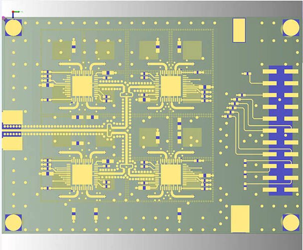
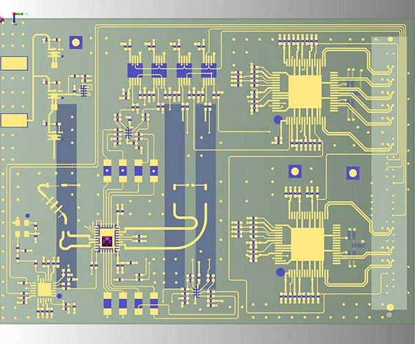
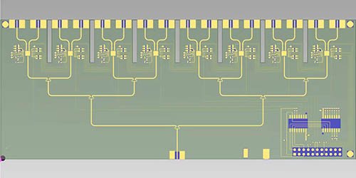
The Design Case